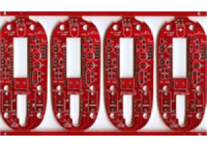
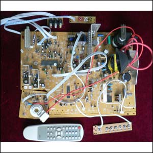
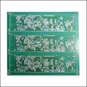
Our main products include: single side, double side, multi-layer PCB, Flexible PCB. Meanwhile, we can also provide a PCB assembly and ODM / OEM servic ... Explore More
Kapton® tapes are polyimide polymers in the form of a film. Kapton® polyimide tapes are also known as high temperature tape or polyimide tape.
Som ... Explore More
.The ESD material is an integral part of the G10/FR4 glass epoxy base.
.The surface resistivity can be supplied to the users specification.
.It of ... Explore More
We produce high quality transformer board ( pre compressed pressboard ),which is applied to produce oil-immersed transformer as insulation material Explore More
Products range-single-sided, double side & multi-layer PCBs and PCB Assembly supply.
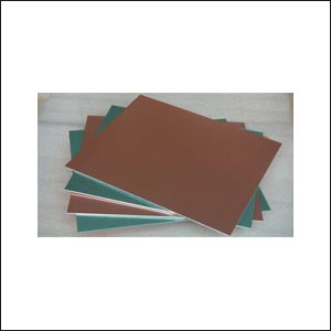
2. CEM-1, FR-4, FR-4 High TG, Aluminum base material
3. PCB O ... Explore More
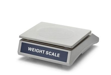
Weighing Machine in Chemistry Lab
They consist of a beam with a friction-free fulcrum, a pointer which attaches to the beam and amplifies deviation ... Explore More
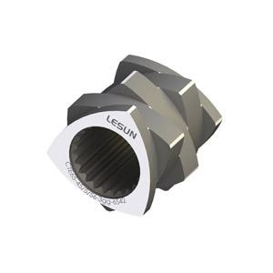
Diameter:
f20 mm ~f300 mm
Properties:
Wear-resisting, Corrode-resisting, Durable
The twin screw extruder elements is self-sweeping type, open long ... Explore More
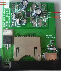
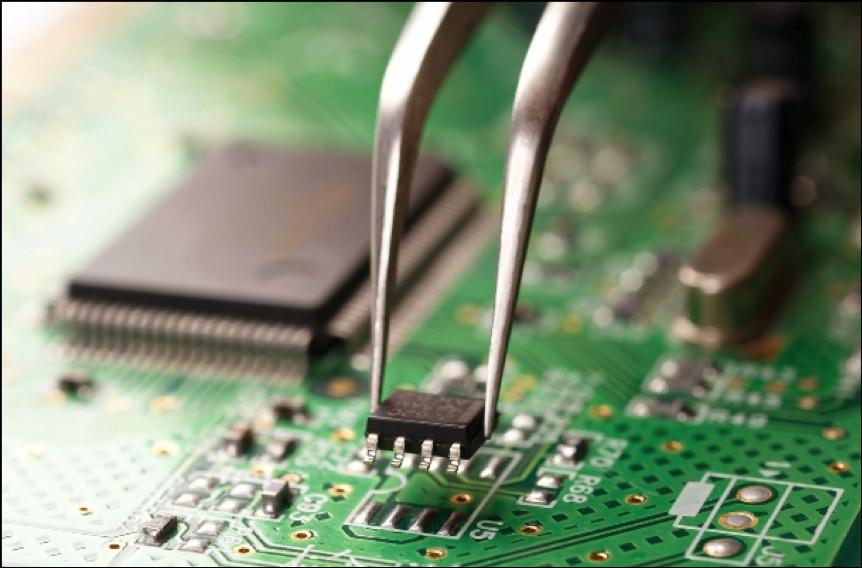
Kingford PCBA is your one-stop supplier of printed and assembled circuit boards. Providing the EMS services to worldwide customers with expert design, ... Explore More
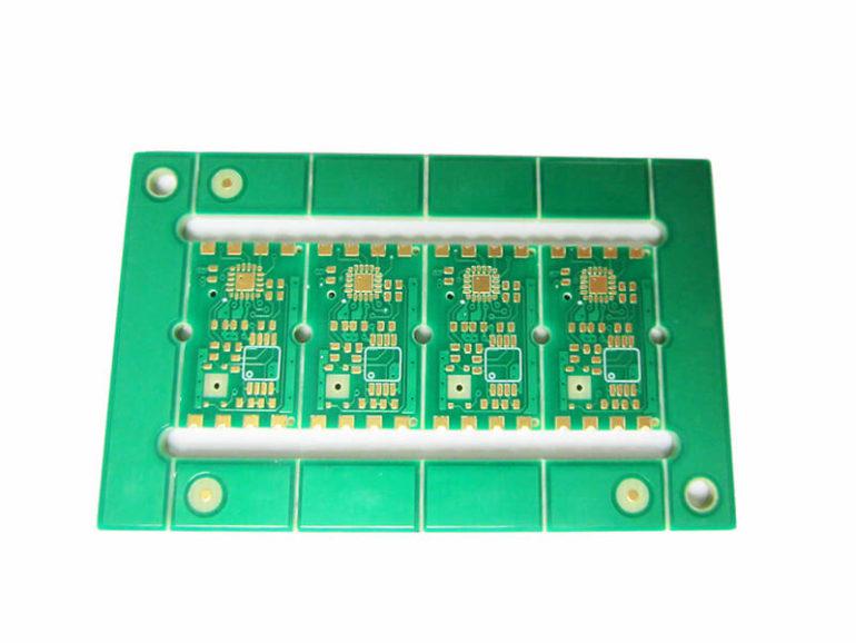
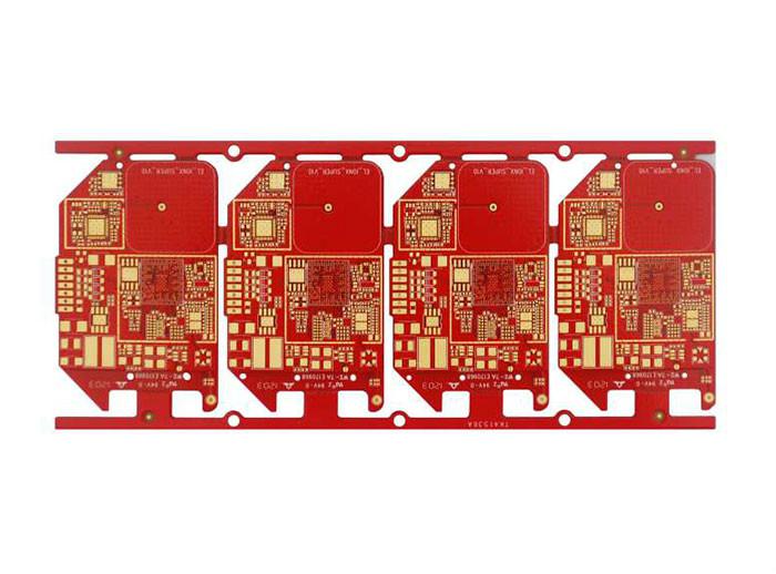
Project Description
| Parameters
4 Layer
Thickness: 1.8+/-0.18 mm(High Tg S1000-2 Material)
Min Hole Size: 0.2 mm
Width/Space: 0.15mm/0.12 mm
Su ... Explore More
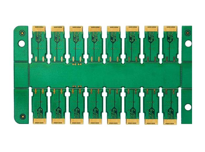
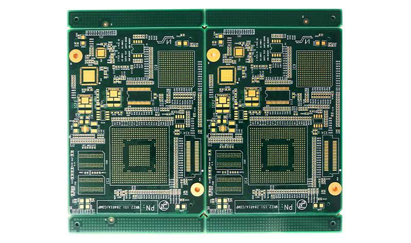
Project Description
| Parameters
6 Layer
Thickness: 1.8+/-0.18 mm
Min Hole Size: 0.25 mm
Width/Space: 0.2mm/0.2 mm
Surface Treatment: ENIG
| ... Explore More
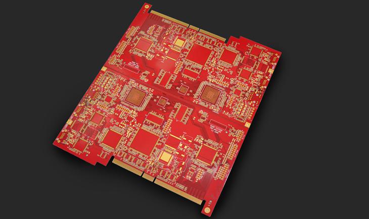
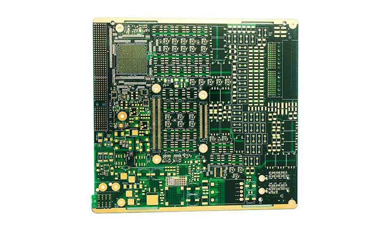
Project Description
| Parameters
10 Layer
Thickness: 1.6+/-0.16 mm
Min Hole Size: 0.15 mm
Width/Space: 0.12mm/0.1 mm
Surface Treatment: ENIG+Go ... Explore More
Project Description
| Parameters
4 Layer
Thickness: 1.2+/-0.12 mm
Min Hole Size: 0.3 mm
Width/Space: 0.12mm/0.12 mm
Surface Treatment: ENIG
... Explore More